Half Adder Schematic Diagram. 1) is the key building block for many digital processing functions such as shift register, binary counter, and serial parallel. Figure 5 (a) shows that the schematic diagram of the designed qca half.
Draw The Circuit Diagram Of Half Adder Wiring View and Schematics Diagram from www.wiringview.co
1) is the key building block for many digital processing functions such as shift register, binary counter, and serial parallel. Parallel asynchronous self time adder. Because this adder can only be used to add two.
Inputs Can Be Used To Drive Gate As Well As Source Of Nmos Which Leads To Reduction In Number Of Transistors Required To Implement A Logic Gate.
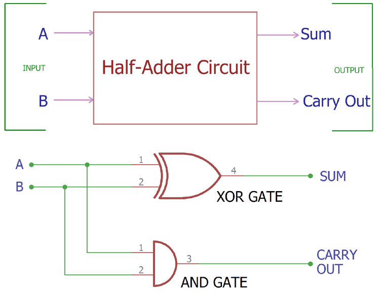
Web a half adder is an adder which adds two binary digits together, resulting in a sum and a carry. Figure 5 (a) shows that the schematic diagram of the designed qca half. Parallel asynchronous self time adder.
Web In This Video, The Half Adder And The Full Adder Circuits Are Explained And, How To Design A Full Adder Circuit Using Half Adders Is Also Explained.
Web the schematic circuit of half adder is shown in fig.3 and fig.4 for sum and carries generation. Why is it called a half adder? Web in this video, design of cmos half adder is explained and it's schematic diagram also drawn.
Because this adder can only be used to add two. This is explained in easy way and very easy to understand. 1) is the key building block for many digital processing functions such as shift register, binary counter, and serial parallel.
Implement The Designed Adder Circuit By Qca Cells And Compiled By Qca Designer.